We use cookies to enhance your experience. By continuing to browse this site you agree to our use of cookies. More info.
Jérôme Pollak, Business Development Director at Tekna Plasma Systems, spoke to AZoNano about commercializing boron nitride nanotubes for advanced materials applications. AlN
For 25 years, Tekna has been developing and commercializing both equipment and processes based on its induction plasma proprietary technology. Our induction plasma technology is especially well adapted to the production of advanced materials and the powders necessary for new innovative emerging products and manufacturing technologies.
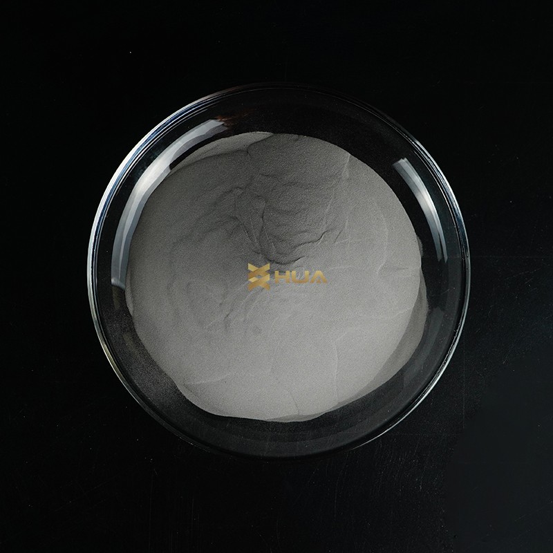
Tekna supplies full-scale productions of a variety of Nano powders and micron-sized spherical powders meeting all the requirements of the most demanding industries. Boron Nitride Nanotubes (BNNT) represent the brand new family of materials at Tekna.
Introduction to TEKNA’s products and services
The National Research Council of Canada (NRC) developed, on a Tekna plasma system, a process to produce Boron Nitride Nanotubes (BNNTs). BNNTs are a material with the potential to create a big turning point in the market. Since last spring, Tekna has been in an exclusive 20-year agreement with the NRC to allow the firm to manufacture Boron Nitride Nanotubes at full-scale production.
BNNTs are an extraordinary material with unique properties that will revolutionise engineered materials across a wide range of applications including in the defence and security, aerospace, biomedical and automotive sectors. BNNTs have a structure very similar to the better known carbon nanotubes. They share the extraordinary mechanical properties of Carbon Nanotubes but have many different advantages.
The structure of Boron Nitride Nanotubes is a close analog of the Carbon Nanotubes (CNT). Both CNTs and BNNTs are considered as the strongest light-weight nanomaterials and are very good thermal conductors.
Although, compared to CNTs, BNNTs have a greater thermal stability, a better resistance to oxidation and a wider band gap (~5.5 eV). This makes them the best candidate for many fields in which CNTs are currently used for lack of a better alternative. I expect BNNTs to be used in transparent bulk composites, high-temperature materials (including metal matrix composites) and radiation shielding.
Comparison between the main properties of BNNTs and CNTs (Source: NRC)
The applications involving BNNTs are still in their very beginning, essentially because of the limited availability of this material until 2015. With the arrival on the market of large supplies of BNNT from Tekna, the scientific community will be able to undertake more in-depth studies of the unique properties of BNNTs which will accelerate the development of new applications.
Many applications can already be envisioned for Tekna’s BNNT powder as it is a multifunctional and high quality material. I can tell you that, currently, the combination of high stiffness and high transparency is being exploited in the development of BNNT-reinforced glass composites.
Also, the high stiffness of BNNT, along with its excellent chemical stability, will make this material an ideal reinforcement in polymers, ceramics and metals.
Besides, many applications where heat dissipation is critical are desperately in need of materials with a very good thermal conductivity. Tekna’s BNNTs are the best allies to improve not only the thermal conductivity but also maintaining a clear colour, if needed, thanks to their high transparency.
Other intrinsic properties of BNNTs are likely to promote interest for the integration of BNNTs into new applications. BNNTs have a good radiation shielding ability, a very high electrical resistance and an excellent piezoelectricity.
TEM image of Tekna's BNNT-R product
Please click here if you would like more information on the instrument used in this article or a quote
BNNTs were first synthesized in 1995. Since then, several other processes have been explored such as the arc-jet plasma method, ball milling-annealing, laser ablation pyrolysis and chemical vapour deposition.
Unfortunately, these processes share a major limitation: their low yield. Such methods result in a low BNNT production which is typically less than 1 gram per hour. This fault is sometimes coupled with the inability to make small diameters (< 10 nm).
As a result, the availability of large quantities of high quality BNNTs for applications development using these processes is still a significant challenge.
Fortunately, Tekna’s inductively coupled plasma (ICP) technology has successfully overcome this challenge. The combination of Tekna’s ICP expertise and its partnership with the NRC opened the door to a brand new range of systems capable of producing highly pure BNNTs in significant quantities. Tekna’s system productivity reaches up to 2 orders of magnitude higher than any of the current methods.
The productivity and cost efficiency of Tekna’s ICP technology allow for the first time, the supply of kilograms of Boron Nitride Nanotubes, produced at a much lower production cost.
The main interesting characteristics include the tube diameter, about 5 nm, and purity (> 50 %). Most nanotubes contain 3 to 5 walls and are assembled in bundles of a few nanotubes.
TEM image of Tekna's BNNT-R product
As large quantities are now available, we saw the launch of several R&D programs based on Tekna’s BNNT, and as much higher quantities will be reached in the next 5 years, we can only imagine what the impact could be in the sciences and industry fields.
You can find information about Tekna and BNNT on Tekna’s website and on our BNNT-dedicated page.
Jérôme Pollak was born in Grenoble, France in 1979. He received the B.Sc. degree in physics from the Université Joseph Fourier, Grenoble. He moved to Québec (Canada) in 2002 to work for the company Air Liquide in the design of plasma sources for the detoxification of greenhouse gases.
He continued his studies in Montreal, where he received an M.Sc. and then a Ph.D. degree in plasma physics from the Université de Montréal in 2008. His M.Sc. thesis was on the design and modelling of field applicators to sustain plasma with RF and microwave fields. While his Ph.D. thesis concerned the plasma sterilization of thermosensitive medical devices such as catheters. He was further involved in the characterization and modelling of cold plasma effects on microorganisms and polymers.
After his Ph.D., he worked for 3 years for Morgan Schaffer in Montreal on the development of gas chromatographic systems using plasma detectors.
Since 2010, he has worked at Tekna Plasma Systems in Sherbrooke (QC, Canada) as an R&D coordinator, then as product and service manager and now as business development director for America. He has been in charge of various R&D projects and business development activities implying micro-sized powder treatment and nanoparticle synthesis by high temperature plasma.
Disclaimer: The views expressed here are those of the interviewee and do not necessarily represent the views of AZoM.com Limited (T/A) AZoNetwork, the owner and operator of this website. This disclaimer forms part of the Terms and Conditions of use of this website.
Alexander has a BSc in Physics from the University of Sheffield. After graduating, he spent two years working in Sheffield for a large UK-based law firm, before relocating back to the North West and joining the editorial team at AZoNetwork. Alexander is particularly interested in the history and philosophy of science, as well as science communication. Outside of work, Alexander can often be found at gigs, record shopping or watching Crewe Alexandra trying to avoid relegation to League Two.
Please use one of the following formats to cite this article in your essay, paper or report:
Tekna Plasma Systems. (2023, August 17). Commercializing Boron Nitride NanoTubes (BNNTs) for the Advanced Engineering Materials Industry. AZoNano. Retrieved on October 12, 2023 from https://www.azonano.com/article.aspx?ArticleID=4144.
Tekna Plasma Systems. "Commercializing Boron Nitride NanoTubes (BNNTs) for the Advanced Engineering Materials Industry". AZoNano. 12 October 2023. <https://www.azonano.com/article.aspx?ArticleID=4144>.
Tekna Plasma Systems. "Commercializing Boron Nitride NanoTubes (BNNTs) for the Advanced Engineering Materials Industry". AZoNano. https://www.azonano.com/article.aspx?ArticleID=4144. (accessed October 12, 2023).
Tekna Plasma Systems. 2023. Commercializing Boron Nitride NanoTubes (BNNTs) for the Advanced Engineering Materials Industry. AZoNano, viewed 12 October 2023, https://www.azonano.com/article.aspx?ArticleID=4144.
Do you have a review, update or anything you would like to add to this article?
Moti Segev & Vlad Shalaev
In this interview, AzoNano speaks to Professor Moti Segev and Professor Vladimir Shalaev, who made surprising discoveries about photonic time crystals that challenge existing research and theories.
In this interview, we discuss a new approach to surface-enhanced Raman spectroscopy that utilizes nano-pockets to capture target molecules, ensuring a highly sensitive way to detect chemical processes.
Dr. Yitong Dong has recently been awarded funding to study custom composite nanocrystals, which could help to create advanced quantum communication technologies. Learn more about this project in this interview.
Discover Phe-nx's NANOS, an analytical tabletop SEM that allows for rapid elemental analysis and is easy to install and use.
The Verifire™ interferometer system provides fast and reliable measurements of surface form error.
This article outlines how Unity, Oxford Instruments’ new detector for a revolutionary new imaging technique, can be used to revolutionize imaging.
AZoNano.com - An AZoNetwork Site
Tungsten Carbide Welding Wire Owned and operated by AZoNetwork, © 2000-2023